Wednesday, 31 August 2011

Post 4 02 sensor(air/fuel ratio) display unit

The task that had to be done was to make a circuit that takes the readings from a oxygen(02) sensor, and displays whether the engine is running a rich air/fuel mixture or running a lean air/fuel mixture using LED's to display whether the engine is running lean or running rich.

^Oxygen Sensor^

The 02 sensor measures the level of oxygen in the exhaust pipe and determines whether an engine is running lean or running rich from the readings that the sensor gets and sends to the ECU(electronic control unit). The voltage received from the 02 sensor determines whether the engine is running rich or running lean, the voltages received from the 02 sensor vary from 0-1volt. So when the ECU receives0-0.2 volts, this means that the engine is running lean as there is a high content of oxygen in the exhaust, this is because of low fuel levels being burnt so not all of the oxygen can burn so there is a high level of oxygen left over in the exhaust. So this low voltage tells the ECU to inject more fuel into the combustion chamber. When the voltage received by the ECU from the 02 sensor is around 0.3-0.6 volts this means the engine has reached stoichiometry and is running the perfect air/fuel ratio. When the ECU receives 0.7-1volt this means that the engine is running rich, this causes low oxygen content in the exhaust as most of it has been burnt due to the high level of fuel in the combustion chamber. This tells the ECU that less fuel is required and the ECU injects less fuel into the combustion chamber. When the engine is cruising at set RPM, the 02 sensor will cycle the air/fuel mixture rich and lean very quickly, this is known as closed loop and is designed to reduce harmful emissions.

COMPONENT LIST

The components required for this circuit are, 3 x 1N4001 diodes, 2 x  0.1uF(micro Farads) Capacitors, 1 x 10,000 ohm resistor and 6 x resistors which values have to calculated (this will be shown later on), 1 x 9v1(9.1volt) Zener Diode, 1 x Red LED, 1 x Yellow LED, 1 x Green LED and 1 x LM324 IC(Operational Amplifier)


CALCULATIONS

To calculate the correct resistor size across R2,R3 and R4, the first thing that needs to be done is to minus 0.6 volts from the power supply as the supply has to go through a diode so this would be 12v-0.6v=11.4volts, then 1.8 volts has to be minused from 11.4volts as this is the voltage required to push through the LED's. So this would make 11.4v-1.8v=9.6volts. Then you would divide 9.6 volts by the current required to turn on the LED's which is 9.5mA, this would be done using ohm's law which is R=V/I, so this would be 9.6v/0.0095A=1010 ohms, this is the answer for R2 and R4 but R3, has different value due to the diode before the yellow LED. So this would be 11.4 v-0.6v-1.8v= 9.0volts. This would mean that 9volts is divided by the current required which is, 9.0v/0.0095A=947 ohm's this is the resistor that is required for R3.

R5 would be 11.4 volts minused by 9.1 volts, as this is the voltage required to push through the Zener Diode, so this would be 11.4v-9.1v=2.3 volts. Then that voltage is divide by the current required which is 5.6mA, so this would be 2.3v/0.0056A=411 ohm's. The value for R6 has already been given so that is 10,000 ohm's, next the current had to calculated on the voltage divider circuit using ohm's law which is I=V/R. So since the voltage supply at the divider circuit is 9.1 volts(this is regulated using the Zener Diode), you would then minus 0.63 volts from supply voltage as this is the voltage required after the first resistor. So this would 9.1-0.63=8.47 volts, I=V/R, I=8.47v/10,000ohm's, so the current then equals 0.000847A.

This leaves just R7 and R8 to be worked out. So the resistances are worked out using ohm's law which is, R=V/I, so R7= 0.23 volts as this is the voltage required above R7 divided by the amperage which is 0.000847A. This means that R7=272 ohm's, and R8= 0.63-0.23=0.4 volts(this is the voltage drop) which is then divided by the current. R=V/I, R=0.4v/0.000847A= 472 ohm's.

This is how all the resistors are worked out for this circuit. The wiring diagram can be seen below as a reference to see what has been calculated.

EXPLANATION ON HOW CIRCUIT WORKS


This circuit works by using the 4 operational amplifiers (the IC chip) that each produce different outputs to light up the LED's, the first diode at the 12 volt power source is their to stop current flowing in the wrong direction going back towards the power source. Just before R5 there is a 11.4 volt input going to the chip to power it, this is going into pin 4, R5 is in place to create the 2.3volt, voltage drop in order to create the 9.1 volts of available voltage for the zener diode. This 9.1 volts is then the voltage supply for the voltage divider circuit. The first resistor in the circuit R6 is already been given to us(10,000 ohm's) and this is used to create a 8.47 volt, voltage drop so that there is 0.63 volts of available voltage at pin 5 on the op amp. Then R8 creates a 0.4 volt, voltage drop so that there is 0.23 volts of available voltage at pin 13. There is always a constant 11.4 volts going to the LED's after the first diode (D2). And the capacitors are in place to smooth the signals in the circuit.


The 02 sensor input is wired up to pins 12,9,6 and 3. And the op amps are used as comparitors, when the voltage signal from the 02 sensor is below 0.23 volts the output voltage from pin 14 is 0 volts, this grounds that part of the circuit and causes the green LED to light up. When the voltage exceeds 0.23 volts, then the positive side of the input for the comparitor is greater and the output for pin 14 will be 11.4 volts, this means there will be 11.4 volts on both sides of the green LED (LED6) and the LED will turn off as current cannot flow through the LED to switch it on. With the green LED this will show that the engine is running lean and the ECU will then inject more fuel to richen the mixture(this is when the engine is on closed loop)

With the voltage now being greater than 0.23 volts from the oxygen sensor, this causes the negative input voltage of the comparitor to be higher than the positive input and this causes a 0v output for pin 8 and this causes the yellow LED (LED 5) to switch on as this part of the circuit can now ground. The yellow LED will remain on until the voltage exceeds 0.63 volts. When the yellow LED switches on this shows that the air/fuel ratio has reached lambda or the correct air/fuel ratio of 14.7 parts or air to 1 part of fuel (14.7:1).

When the voltage exceeds 0.63 volts the Red LED (LED1) will switch on, this shows that the engine is running rich and the ECU will then inject less fuel into the combustion chamber (when the engine is on closed loop). The problem with this circuit is that when the Red LED comes on the yellow LED will remain on until the voltage falls below 0.23 volts. So to fix this problem there is an output from pin 1 that sends positive 10.8 volts to the negative side of the LED, so with positive 10.8 volts on the positive side of the diode no current can flow and the yellow LED switches off. And allows the red LED to remain on. The reason that the voltages are 10.8 volts, is that there is the initial voltage drop to get through the first diode of 0.6 volts which brings the available voltage down to 11.4 volts then there is another voltage drop across the diodes D3 and D4. These diodes are put in place as when pin 1 sends a positive output voltage it doesn't blow the send positive voltage back to the voltage supply on the positive side of the LED (D4). And D3 is put in place to stop positve voltage going to the output of pin 1 and blowing the op amp, the diodes are also in place so that the voltages are equalized so that the LED does switch off.

BREADBOARD CIRCUIT

Before the 02 sensor display unit could be put on a PCB board the circuit had to be wired up so that we know how the circuit works by wiring it up ourselves. However problems do occur with wiring up the circuit ourselves, the first problem is that I got the pins 8-14 around the wrong so the circuit would not work, then trying to re-wire the circuit I had a jumper wire going from pin 5 to pin 8 this caused the yellow LED to never light up as this part of the circuit was being by-passed. However the circuit did wind up working in the end as seen in the photos below.


The photos above show the three different LEDs on at different times, when the red LED is on this shows that the 02 sensor input is above 0.63 volts, with the yellow LED on this shows that the 02 sensor input voltage is below 0.63 volts but above 0.23 volts. When the green LED comes on this shows that the 02 sensors input voltage is below 0.23 volts.


PCB CIRCUIT

Once the circuit had been wired up on the breadboard, we could then start soldering the components onto the  PCB. Once the circuit was completed the circuit was tested and then later on a fault was placed so that it could be worked out by a colleague so that they can show understanding on how the circuit works, this fault will be described later on. The finished circuit can be seen below.


FAULTS ON PCB

When a fault is given to you the colleague does not tell you what the fault is, first you have to a visual inspection to check for breaks in the circuit. The break in the circuit I got was on the negative LED leg on resistor R2, this created the fault in which the circuit operated normally except for when the engine runs rich the red LED does not light up. This is because this part of the circuit is not connected to anything so when pin 7 goes to 0volts the LED is not connected and a circuit is not completed so the Red LED will not light up. To repair this fault the leg on the resistor was simply soldered back together to create a circuit.

This would mean that there would be 11.4 volts at the negative side of the LED, and as it cannot connect to earth no current can flow through LED 1 or the Red LED, however the rest of the circuit works as normal. There is still 11.4 volts going to each LED, with 10.1mA of current flowing through each LED which is a good reading (this current was measured). There is still 9.1 volts powering the voltage divider circuit. And there is still 0.87mA of current which is normal (this current was measured). And the 02 sensor input still sends the correct voltages to the inputs of the circuit, except the Red LED will not light up until the resistor was reconnected and a circuit could be created.

FINISHED CIRCUIT

The circuit can be seen working in the video below.

The red LED remains on at the end of the video as the engine was still cold and was therefore still running rich, but it does show the 02 sensor on closed loop running the engine between rich and lean.

REFLECTION

This circuit worked well with minimal problems wiring it up and soldering it, so there is not much that I can improve on it as the soldering was good and generally had minimal problems. The things I learnt from building and testing the circuit is exactly how an op amp works as a comparitor, and how to do good clean soldering, and also how to wire the circuit properly on a breadboard.


REFERENCE
http://www.bmwtips.com/tipsntricks/Exhaust/O2sensor_files/o2sensor1a.jpg(02 sensor Image)

https://blogger.googleusercontent.com/img/b/R29vZ2xl/AVvXsEjkYhSafOWs_7ryazfDlaJxA0E4XUYFKV01v9oWGL2zn5f7ln2gIf5Nj4bOnVwDZJe-YlCFsfSVA860lJMsHjX-EVsj9xgDE9xqaw943EJgG17uE-5cwoBeLueFO2FsBb1R0PN7eRHh9mC9/s1600/op11.png(LM324 data sheet)

http://elcodis.com/datasheet.php?c=1315884&c_name=LM324AN&doc=164605(LM324 wiring diagram)

http://moodle.unitec.ac.nz/mod/resource/view.php?id=74411(02 sensor wiring diagram)

http://www.youtube.com/watch?v=HCCgpnEmBuo(Finished 02 sensor board)

Thursday, 18 August 2011

Fuel Injector Board Circuit. Post 2

The task that had to be done was to wired up components on a PCB board that made LED's light up when a voltage is supplied to the base of the transistor, this causes the LED's to light up and indicates when the fuel injectors are firing.
COMPONENTS
The components that are needed are 4 resistors which can handle a maximum of 0.25 amps at 25 degrees celcius, the values of which have to be calculated. 2 NPN BC547 transistors which can handle a maximum of 45 volts from the collector to the emitter. The maximum voltage through the base is 6 volts and the maximum current through the collector is 200mW, and a maximum reverse voltage of 50volts from the emitter to collector, and a maximum reverse voltage of 50 volts from the emitter to base. All these ratings are for when the transistor is at 25 degrees Celsius, if the transistor is hotter than 25 degrees then the transistors specs are less. Two LED's are needed which can handle a maximum of 180mA when wired up in forward bias, the power dissipation is 684mA and the maximum voltage is can handle is 2.5volts, all these specs are when the LED is at 25 degrees Celsius if the temperature of the component exceeds this then the specs reduce. Then the components are wired up on a bread board to make sure that the circuit works and that we have an idea on how to wire up the components on the PCB board. The calculations for the resistors where used to make sure that the each component was getting the correct amperage to make the transistors and LED's work efficiently. Using a data sheet the amperage that the transistor can operate in was found out so that the correct sized resistor could be used for the pulse signal circuit. The amperage through the base that let the transistor be in the saturated region was 0.5mA so since the amperage is known, and the voltage supply is 5 volts minus the voltage required to turn on the transistors which 0.6 volts. The resistance can be worked out using ohm's law, and the triangle can be seen below.
Ohm's Law Triangle
Ohms Law Triangle Relationship
CALCULATIONS

So to find out resistance the voltage which is 4.4 volts as 0.6 must be minused as that is required to turn on the base side of the transistor, 4.4 is then divided by the amperage (R=V/I) which is 0.005A and this gave an answer of 880 which is the size of resistor required 880 ohm's. But since there was no 880 ohm resistor a 820 ohm resistor was used in the circuit, this is better as it allows a bit more current to flow through the base and lets the transistor be more saturated or turned on so there will be less of a voltage drop through the collector. Which means there is more voltage and current available for the LED so that will be brighter. Then the resistor size was worked for the power side of the circuit that lights up the LED's, the voltage supply is 12 volts but minus the voltage to pass through the LED which is 1.8 volts then minus another roughly 0.2 volts to pass through the collector due to some resistance which is always in the transistor. And the amperage required to turn on the LED is 20mA, so R=V/I, R=10/0.02A so the resistor required was 500 ohm's but since there was no 500 ohm resistor a 560 ohm resistor was used for the bread board circuit. The image below shows the fuel injector circuit wired up on the bread board. I then calculated the current flowing through both the pulse control side of the circuit and the LED side of the circuit. The pulse control current was worked out using ohm's law I=V/R,   I=5volts/820ohm's,    I=0.0061amps, this is how many amps are flowing through the base of the transistor. Then using the same equation the LED circuits current was worked out, I=V/R,     I=12volts/470 ohm's,      I=0.025amps, this is how much current is flowing through the LED

BREADBOARD CIRCUIT
One small problem that was encountered was the 560 ohm resistor was to large for the LED and the LED was not very bright so for the circuit that was going to wired up on the PCB board 470 ohm resistors where going to be used. This will allow for more current to flow through the LED which will make it brighter so that it is more visible when the LED actually lights up.
PCB CIRCUIT
Once the circuit has been wired up on the bread board the circuit then had to be wired up on a program called LochMaster, which allows you to place components and check where the current is flowing and the voltage supply is known so that components are not loaded with to much voltage, this is stopped by putting cuts in the board so that voltage is shared instead of every component getting its own 12 volt supply. The cuts are put on the copper strips between in the middle of components e.g in the middle of a resistor, this puts a break in the circuit and means that the other component can only get the voltage from the first component that has had the voltage drop for example an LED wired up after the resistor can only 1.8 volts power supply as since the resistor consumes the rest. The cuts are simulated on LochMaster, so that these cuts can be placed in the same place on the PCB board, and the other components can be place in the same position as well. Now everything can be placed in the exact same place to make it easy to wire up the circuit, now you just need to look at the LochMaster program to know where to place the components. The injector board circuit is seen wired up on LochMaster below showing where the components have been placed and where the soldering points are on the circuit which can be seen on the board that has been turned upside down.
injector circuit top sideinjector circuit bottom side
^Component Position^                                                 ^Soldering points (Upside down)^

The three positve terminals on the left hand side of the left image are the inputs the top positive terminal is the 12 volt power supply for the LED's. The two lower positive terminals are the 5 volt inputs that switch on the transistor and the entire circuit by allowing current to flow through the base to the emitter. This is the pulse signal which makes the circuit switch on and off, which is what makes the LED's switch on and off. The negative terminal at the bottom of the board is the ground for the entire circuit. The image on the right, above shows the soldering points for the circuit and also shows the cuts made in the board to allow the circuit to work properly.

View Richard.jpg in slide showView photo.JPG in slide showView photo.JPG in slide show
^injector board wired up^                  ^soldering points on board^        ^circuit layout design and working^

The circuits layout and description can be seen below.


EXPLANATION ON HOW CIRCUIT WORKS

The circuit works by having a constant 12 volt power supply which goes to the LED's, this can be seen coming from terminal 1. The LED's will remain off, until a 5 volt power source is given to the base side of the transistors this is from terminal 3 and 4 or PWMO, this then switches on the circuit and allows current to flow from the base to the emitter this then allows current to flow from the collector to the emitter, current can then flow from the 12 volt power source, through the LED's and to earth, this then turns the LED's on. Then when the pulse signal from the 5 volt supply is switched off again the whole circuit is switched off again as current cannot flow through the LED's until the base side of the transistor is switched back on again from the 5 volt pulse supply, then current can flow from the base to the emitter, which in turn allows current to flow from the collector to the emitter which turns the LED's back on again. This pulsing signal comes from the fuel injectors and is meant to represent the fuel injectors on time which is shown when the LED is on and when the fuel injector is off then the LED is off.

TESTING PROCEDURE

Before the circuit was checked and wired up to the 12 volt power supply and the function generator which creates the pulsing 5volt signal which switches the LED's on and off using a duty cycle of 50% on and 50% off. The board was tested to make sure all the components where still working. This was done using a multimeter, first I set the multimeter to ohm's and checked that there was continuity through the input wires from the 12 volt power source and the 5 volt pulse signal wires and through the earth wire, and there was with almost no resistance of 0.02 ohm's which was expected. If there was a high resistance reading this would mean that there could be a bad connection caused by poor soldering, this would cause resistance and voltage would be used up to pass through this resistance this would mean that there is less voltage and current for the LED's to use or less voltage and current for the transistor to switch on properly. This could cause one of the LED's to be duller than the other as it is not getting enough current and voltage to switch on properly. If the resistance was on the control side of the circuit or where voltage flows through the base this could mean that the transistor is not saturated so the collector side is not switched on properly causing a voltage drop across the collector to the emitter and the LED will not switch on properly as some voltage and current is being used up. I tested the wires connections on the solder side of the circuit to make sure that poor soldering was not affecting how the circuit operated.

Then I tested the continuity through the jumper wires with the multimeter still set to ohm's, the jumper wire which supplies 12 volts the LED's and the one that grounds the circuit. If either of these did not work due to high resistance then the LED's may not switch on properly or if the jumper wire to ground did not work then the circuit would not work as current cannot flow and the LED's would not light up. However both jumper wires had minimal resistance with both producing 0.02 ohm's resistance, once again high resistance could be caused by poor soldering. I tested this on the solder side of the circuit to make sure that solder did not affect the circuit operation

I then set the multimeter to diode test mode and checked that the LED's still switched on, which they did switch on with 1.75 volts, this is a good reading, if the Multimeter showed there was open circuit, this could mean that the LED was blown because it was overheated when the solder was being placed as the soldering iron heated the component to long this would mean that the LED would have to be replaced. Or it could mean that poor soldering has caused to much resistance in the circuit and the multimeter cannot switch on the LED, this would mean that the LED would not light up properly and it might not light up at all as not enough current can flow. I tested the LED's on the solder side of the board so that I know if the solder is affecting the operation of the LED's.

Leaving the multimeter set to diode test mode, I then tested the transistors base side of the circuit and the collector side of the circuit, all on the solder side of the circuit so that I know whether solder is having any affect on the operation of the board. Both transistors gave a reading of 0.6 volts on the base side which is a good reading, and both gave a reading of 0.7-0.8 volts on the collector side which is a good reading. A bad reading would be open circuit as this would indicate that the transistor was overheated by the soldering iron when the solder was being placed and this caused the transistor to blow up, and stop working this would mean that the transistor would have to be replaced.

PROBLEMS

The only small problem that was encountered was when the circuit was wired up on the bread board, a 560 ohm resistor was used on the LED side of the circuit and this was to big and did not let enough current through the circuit. This meant that the LED's where dull, so when the circuit was wired up on the PCB board, 470 ohm resistors where used to allow more current to flow through the LED's and make them brighter, so that it was more visible that they where operating.

REFLECTION

The biggest problem I faced in making this circuit was making good soldering connections, so if I could do this  circuit again then I would have more practice at soldering components before I wired up the circuit so that there wouldn't as many bridges made when I was soldering. (Bridging is when solder connects to components that should not be connected together and could even be connected from separate tracks, this would cause major problems with the circuit as this could give voltage supplies to the wrong components and over load the circuit with to much current and voltage.

REFERENCE:
datasheet for transistor http://www.datasheetcatalog.org/datasheet/MicroElectronics/mXuwzwr.pdf

datasheet for LEDhttp://www.lunaraccents.com/educational-LED-bulbs-data-sheets-absolute-ratings.html

(ohm's law chart)http://nz.images.search.yahoo.com/images/view?back=http%3A%2F%2Fnz.images.search.yahoo.com%2Fsearch%2Fimages%3Fp%3Dohms%2Blaw%2Btraingle%26ei%3DUTF-8%26fr%3Dyfp-t-501&w=469&h=182&imgurl=www.electronics-tutorials.ws%2Fdccircuits%2Fdcp23.gif&rurl=http%3A%2F%2Fwww.electronics-tutorials.ws%2Fdccircuits%2Fdcp_2.html&size=9KB&name=Ohms+Law+Triangl...&p=ohms+law+traingle&oid=e7a5feb7731ee5257cfdc33a9a9dcf59&fr2=&spell_query=ohm%27s+law+triangle&no=1&tt=169&sigr=11pp7s5bi&sigi=11h5vl4tj&sigb=12pgie892&type=gif&.crumb=HHVRhjVZ21c

Post 3 Electrical Components and calculations

Electrics and electronics are used for just about everything, in this blog I'm going to talk about how certain electrical components work and how electricity or current actually flows and how to measure voltages on components, and how to do calculations to work out how much voltage is required or how much current  there will be in a circuit or the resistance and many other calculations that are required to work out certain aspects of an electrical circuit

.
BASIC ELECTRICS
First I'm going to talk about conventional electricity and electron theory, as these are major aspects to understanding electricity. Conventional current flow is when current flows from the positive power source for example a battery to the negative terminal of that battery, this is what is shown in all wiring diagrams. This is not correct as current or electrons actually flow from a negative terminal to a positive terminal, and this is known as electron theory or flow. However there is some truth to conventional current flowing from positive to negative as an atom especially good conductors i.e atoms with 1 or 2 electrons in the outer shell, leave positively charged holes in place of the electron, so spare electrons which are negatively charged, could jump from another atom to fill the spare hole and this happens to flow in the direction of conventional current flow from positive to negative. This has only recently been worked out as it was presumed that electricity flowed from positive to negative "In the 19th century, with the early applications of electricity such as starter motors and light bulbs, there was not an exact understanding of the nature of current flow. It was assumed at the time
that electricity flowed from the positive terminal to the negative." This is most likely the reason why wiring diagrams state that current flows from positive to negative, as it has been presumed that current flows this way for so many years that it would be to difficult to change and also that it easier to comprehend that current flows from positive to negative. 


Now how to do calculations on a simple circuit.


For this circuit, the amperage is going to worked out as the voltage supply is known and the resistance is known. The voltage current and resistance can be worked out using the triangle below.


I=V/R
I=4.4v(this is because the diode requires 0.6v to turn on)/10 ohm's
I=0.44Amps.

You can also work out power dissapation across the diode using the equation triangle below.

So power dissapation across the diode = voltage x amperage so P=0.6v x 0.44amps
                                                                                                 P=0.264 watts
and the power dissapation across the resistor would be P=0.44amps x 4.4v
                                                                                    P=1.936 watts

These are some easy equations to work out some of the different aspects of a electrical circuit.

VOLTAGE DIVIDER CIRCUIT

A voltage divider circuit, will provide a constant set voltage supply to a consumer that is always less than the supply voltage, for example if the power supply is 5volts, then a voltage divider circuit can supply a constant voltage of 3 volts to a consumer.


To work out what Vout is for the voltage divider circuit, you need to know what the resistors are in the circuit. So for example the resistors could be, R1=970 ohm's, R2=4700 ohm's, R3= 100 ohm's, the equation used to work out what Vout1 is Vout=R2 + R3/RT x Vin, so that would be Vout=4700 + 100/5770 x 12volts, this means that Vout 1= 9.98volts. Then to work out Vout2 that would be, Vout=R3/RT x Vin, Vout=100/5770 x 12, Vout2= 0.2 volts. These are the steps required to work out what the output voltages would be.

But if you want to pick what the voltage is for voltage divider circuit, for example you want a constant 4volts from a 5volt source for Vout1 and a constant 0.2 volts for Vout2 as an example. Then you would have to pick the first resistor(R1) and it can be any sized resistor, so for example a 1000 ohm resistor. Now you can work out the amperage is by calculating the voltage drop across the first resistor which would be 5volts-4volts=1volt, this means that I=V/R, I=1volt/1000 ohm's, I=0.001 amp. To work out what size the second resistor is (R2) you minus the available voltage by the voltage required at Vout2 this would be 4volts-0.2volts=3.8 volts and to work out resistance you divide voltage by current R=V/I, R=3.8volts/0.001amps, so R2=3800 ohm's. And to work out R3 is, the voltage required at Vout2 is divided by the current, R3=R=V/I, R=0.2/0.001amps, so R3=200 ohm's. This will then give a constant 0.2 volt supply from Vout 2.


OPERATIONAL AMPLIFIER

An operational amplifier(op amp) is a high gain electronic component(gain being the difference between the input and output voltages), the operational amplifier will take a small input voltage for example a 2volt input and can produce a higher output voltage for example 12 volts, or it can produce a negative or 0 volt when wired up as a comparitor but that will be explained later on. First the non-inverting op amp will be explained, the non-inverting op amp uses a small voltage input for the positive input side and produces a larger positive output voltage. This can be worked out using the equation Vout= ((Rf/Rs)+1)xVin, so if the input voltage is known and the resistors are known then Vout can be calculated.
So for example if Vin is 0.05 volts and Rf is 47kohm and Rs is 1k ohm then Vout can be calculated, Vout=((47000/10000)+1)x0.05, this would make Vout 2.4 volts.

INVERTING OP AMP

An inverting op amp works in a similar way to the non-inverting op amp except that the output is negative, the inverting op amp receives a small input voltage for the negative side of the op amps input, and if the op amps voltage rail is wired up to a negative voltage then the output would be a larger negative voltage than the voltage input. If the op amp is not wired up to a negative voltage and is only wired to ground or 0 volts then the output will be 0 volts. This circuit can be used as a negative switching circuit to switch components on and off on the negative side of the circuit. Whereas the non-inverting op amp can be used as a positive switchingcircuit. Vout can be worked out using the following equation, Vout=(Rf/Rs) x  -Vin.

COMPARITORS

A comparitor is an operational amplifier that compares two input voltages and which ever is the biggest voltage will be the output. For example if there was a 2 volt source going to the inverting input and a 1.5 volt source going to the non-inverting input, then the output would be negative whatever the voltage is at the voltage rail. If these where switched around then the output would be a positive output to whatever the voltage rail is connected to, for example positive 12 volts. Here are some comparitor examples below.

This means that a comparitor can be used to ground a circuit or to provide voltage to a consumer. And this is why operational amplifiers are so popular in electrical circuits, however an operational amplifier can not produce a greater voltage than what is supplied at the voltage rail. For example, if you had 12 volts at the voltage rail and 20 volts at the inverting or non-inverting input, the output would only be 12 volts as the op amp cannot create more voltage than what it is supplied with.


MOSFETS

Mosfet's or metal oxide semi-conductor field effect transistors, are much like the normal BJT (Bipolar junction Transistor), in that both require a small input to switch on a larger output, and that both have two different types of transitors. The normal BJT has NPN and PNP and the MOSFET has a  P-channel and a N-channel. However there are quite a few differences. For one the BJT is a current controlled device although there is a voltage drop that is required to switch on the transistor it is the amount of current that determines how well the transistor operates, in that a small amout of current is required flowing from the base to the emitter to switch on a larger current from collector to the emitter for a NPN transistor, a PNP transistor requires zero amperage to switch on. The MOSFET is a voltage controlled device in that for a N-channel FET(Field Effect Transitor), the more voltage that is applied to the gate (which is like the base on a BJT), the less resistance there is to voltage and amperage flowing from the drain to the source. However this is different for the P-channel FET , the more negative voltage that is applied to the gate the less resistance there is to voltage and current flowing, much like a PNP transistor.


Within the to different channels for a MOSFET there are two different types of MOSFETs, there is the enhancement type, which is seen in the above image, this type of MOSFET "requires a Gate-Source voltage, ( VGS ) to switch the device "ON". The enhancement mode MOSFET is equivalent to a "Normally Open" switch."  The other type of MOSFET is known as the depletion type MOSFET this type requires  "the Gate-Source voltage, ( VGS ) to switch the device "OFF". The depletion mode MOSFET is equivalent to a "Normally Closed" switch." The depletion type MOSFET can be seen below.


Like the BJT the MOSFET also has a saturated region and a Cut-off region which are exactly the same for both MOSFETS and BJT's, in the saturated region the MOSFET has the correct amount of voltage at the gate to make it fully switch on. And when the voltage at the gate falls below a certain point then the MOSFET switches off, this is the cut-off region. The pros and cons of the MOSFET and BJT can be seen in the table below.


 Field Effect Transistor (FET)Bipolar Junction Transistor (BJT)
1Low voltage gainHigh voltage gain
2High current gainLow current gain
3Very input impedanceLow input impedance
4High output impedanceLow output impedance
5Low noise generationMedium noise generation
6Fast switching timeMedium switching time
7Easily damaged by staticRobust
8Some require an input to turn it "OFF"Requires zero input to turn it "OFF"
9Voltage controlled deviceCurrent controlled device
10Exhibits the properties of a Resistor 
11More expensive than bipolarCheap
12Difficult to biasEasy to bias


The reason that the MOSFET is a voltage controlled device is that there is extremely high resistance at the gate of the MOSFET so there is almost no current flow through the gate to source, but this means that there is high amperage and voltage flowing from the drain to source. The MOSFET has an advantage over the BJT in that the MOSFET can handle much higher voltages and amperage than a BJT of the same size. However is seen in the chart above the MOSFET is easily damaged by static electricity that is generated by the body, the reason the MOSFET gets damaged is that the gate on the MOSFET acts like a capacitor and stores a charge in the gate, this damages the oxide in the gate and renders the MOSFET useless. To stop the MOSFET being damaged by static electricity, you must ground yourself when handling the MOSFET as this will stop static electricity accumulating on the body and damaging the MOSFET.

These are some of the basic electrical components that are used every day and the calculations that are required to work out the different vital aspects of an electrical circuit to make it work properly and effectively.


REFERENCE:
http://www.talktalk.co.uk/reference/encyclopaedia/hutchinson/m0030248.html(conventional current flow quote) 
http://cyberchalky.files.wordpress.com/2010/03/web_ohms_law_triangle.gif  (ohm's law triangle)
http://www.electronics-tutorials.ws/dccircuits/dcp24.gif(power triangle)
http://www.markallen.com/teaching/images/electronics/comparator.jpg(comparitor image)
http://www.acdcshop.gr/img/components/transistor_fet/fet/3197_irfp4227pbf.jpg(mosfet image)
http://simreal.com/mediawiki/images/2/26/Fig06-02.jpg(P and N channel MOSFET enhancement image)
http://www.electronics-tutorials.ws/transistor/tran_6.html(quote for enhancement type MOSFET)
http://www.electronics-tutorials.ws/transistor/tran_6.html(quote for depletion type MOSFET)
http://electricalandelectronics.org/wp-content/uploads/2008/09/symbol-of-depletion-type-mosfet.png(depletion MOSFET Image)
http://www.electronics-tutorials.ws/transistor/tran_8.html(BJT/MOSFET comparison table)

Saturday, 13 August 2011

TTEC 4847 Automotive Electronics

EXPERIMENT NO.1

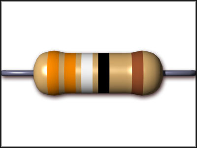
The first task that had to be done was to learn how to check the resistances of different resistors and know what there resistances are by using the Resistor Colour Code Chart. This chart will help you to decide what the resistance of different resistors by looking at the order of the stripes on that resistor for example if you see a gold or silver stripe which most resistors have this is there tolerance, this is always the last stripe to check. The chart that is used to check resistances is seen below. The chart is used so that the resistance can be calculated by looking at the chart. To find out the resistance of a resistor you look at the resistor so that the  tolerance or the gold/silver stripe is on the right hand side this helps to make it easier to calculate the resistance, the first two or three stripes are the numbers to note, in most cases its only the first two stripe numbers that have to be noted, the next band is the multiplier this is how much the numbers need to be multiplied by . The last band is the tolerance this is how much the resistance can vary by from the what the resistors resistance is meant to be this is usually 5-10% or the gold or silver stripe. For example a resistor with the stripes brown, black, yellow and gold. This would mean that the number would be 10 then the multiplier would be x10,000 this would make the resistance 100,000 ohm's and the gold stripe would be how much this would actually vary. So the resistance could be as high as 105,000 ohms down to 95,000 ohm's. Then setting a multimeter to ohms you would then measure the resistance to make sure that the resistor is still good to use as if the resistor is not within these specifications then it is faulty and should not be used.
 
The first task that had to be done was to calculate how much resistance a resistor and calculate there tolerances, then measure the resistor with a multimeter to make sure the calculations were correct.

VALUE (COLOUR CODES)                                          (VALUE MULTIMETER)
-56x100=5600 ohm's
tolerance=5% 5600x1.05=5880 ohm's                                5.53k=5530 ohm's
                      5600x0.95=5320 ohm's

-10x10,000=100,000 ohm's
tolerance=5% 100kx1.05=105k ohm's                                98.6k=98,600 ohm's
                      100kx0.95=95k ohm's

-27x10=270 ohm's
tolerance=5% 270x1.05=283.5 ohm's                                 266.2 ohm's
                      270x0.95=256.5 ohm's

-470x1=470 ohm's
tolerance=5% 470x1.05=474.7 ohm's                                 459 ohm's
                      470x0.95=446.5 ohm's

-10x1k=10,000 ohm's
tolerance=5% 10,000x1.05=10500 ohm's                           9.84k=9840 ohm's
                      10,000x0.95=9500 ohm's


A bad reading whilst using the multimeter would be one that is completely different to the resistance that was calculated using the resistor chart or even if it is just out of the specification for the resistor this means that it is faulty and should not be used. For example if you had a 5600 ohm resistor but the reading you got for the resistor was 6000 ohm's you should not use it as it is not the correct resistance and could affect the operation of a circuit that it is in as it could be resisting to much current flow for example this would mean that another component may not operate properly as it is not getting enough current for it to operate this could be a transistor for example. However all the readings that were taken down for this experiment where good as they were all within specification.

The next part of the experiment was to choose to resistors with different resistances and measure them with the multimeter so that exact resistance can be known.

Resistor 1: 5530 ohm's                                               Resistor 2: 9840 ohm's

Then the resistors where put in series and the resistance was calculated then the total resistance was measured.

Calculated value 1 and 2 in series : RT=R1+R2: 5530 + 9840 = 15370 ohm's

Measured value 1 and 2 in series : 15490 ohm's

Next the resistors where wired up in parallel this is done by twisting the ends of the resistors together then the resistance was calculated and then measured.

Calculated value 1 and 2 in parallel: 1/RT=1/R1+1/R2+1/R3: = 3549 ohm's

Measured value 1 and 2 in parallel: = 3420 ohm's

What principles of electricity have been demonstrated with this? Explain


The purpose of the resistor is to reduce current flow so that damage does not occur to components in the circuit. The value of a resistor means how much effort is required to push through it, e.g the higher the resistance the greater the effort required to get through the resistor. When two or more resistors are wired up in series the total resistance is added together from each resistor to make the overall resistance resistance in that circuit this can be worked out using this equation, RT=R1+R2+R3. If the resistors are wired up in parallel then the total resistance of the circuit is lower than the lowest valued resistor.This is because high amperage is required to give each component there own power source so low resistance is needed to achieve this high amperage.


EXPERIMENT 2

Diodes


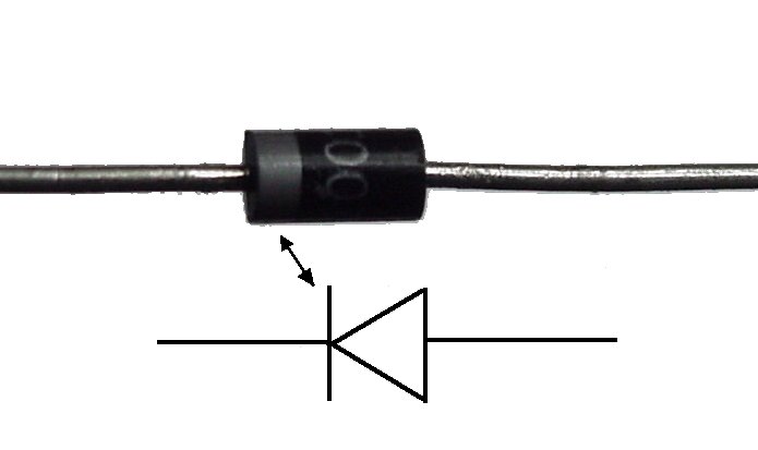
The purpose of a diode is to allow current to flow in only one direction which is forward bias, if current tries to flow the other way it will incounter a binary layer that prevents current from flowing in the wrong direction. This circuit could be used to convert alternating current into direct current. This is used on alternators which produce alternating current, it is then turned into direct current so that the battery can receive charge as if the battery received alternating current it would not charge as the voltage would simply exit the battery again just after it entered the battery. All diodes required 0.6 volts to turn on and allow current to flow in the circuit and in the desired direction


A diode has the characteristics of:
-An insulator when current tries to flow in one direction
-A conductor when current flows in the direction

Exercise: Using a multimeter, identify the anode and cathode of the diode and the LED


Voltage drop in forward Biased Direction.
Voltage drop in reverse biased direction
LED
 1.783 volts
 O.L(open circuit)
Diode
 0.564 volts
 O.L(open circuit)


Explain how you could identify the cathode without a multimeter 


On an LED the anode or positive leg is always longer than the cathode or negative leg. On a normal diode the cathode or negative side has a stripe on it so that the polarity of the diode can be known this is the only way to identify the anode and cathode side of the diode. If the legs have been cut on the LED and are the same length then look at the top of the LED and you will see a flat side this is the negative side of the LED.

Exercise: For Vs=5v, R=1k ohm's, D=1N007 build the following circuit on a breadboard.


Calculate first the value of current flowing through the diode, now measure and check your answer?
show your working.

Calculated                                                                                      Measured
-I=V/R                                                                                          0.0045Amps
-I=5v/1000 ohm's=0.005Amps

Is the reading as you expected; explain why or why not?

-Yes the reading is what was expected as ohm's law was used to calculated the amperage (I=V/R) and the amperage is low because of high resistance from the circuit being wired up in series.

Measure the voltage drop across the diode. (can not calculate it as ohm's law cannot be used to calculate)

-Measured
0.672 volts


What is the maximum value of the current that can flow through the given diode?
-The diode can handle 1.0amps max at 75 degrees celcuis, this value can be greater when the diode is at lower temperatures.

For R=1k ohm's. What is the maximum value of Vs so that the diode operates in a safe region?
-Any voltage that is 999.4 volts or less as the diode can only handle 0.6 volts and the resistor and can consume the rest of that voltage.

Replace the diode by an LED & calculate the current, then measure and check your answer?

Calculated                                                                                     Measured
I=V/R                                                                                           0.003Amps
I=3.2volts/1000 ohm's
I=0.0032 Amps

What do you observe? Explain Briefly.
-The LED requires a high voltage to turn on, as opposed to the diode. This means that current is lower as more load is on the circuit to push current through the LED to switch it on. And since the diode requires less voltage to turn on this puts less load on the circuit and hence current flow is higher.

Things that can go wrong with diodes is that they can be overloaded with either to much voltage or to much current or both. When this happens the diode creates an open circuit so current cannot flow this means that the circuit that the diode is in will not operate if the circuit is in series.

EXPERIMENT No.3
Components: 2 x resistors, 1 x 5V1 400mw Zener diode (Zd)

Exercise: Obtain a breadboard, suitable components from your tutor and build the above circuit.

For R=100 ohm's and RL=100 ohm's, Vs= 12v

What is the value of Vz
-Vz is 4.96volts, this is the voltage drop when the power supply is at 12 volts.

Vary Vs from 10v to 15v
what is the value of Vz

When the voltage was at 10v the value of Vz or the voltage drop across the zener diode was 4.84 volts, when the voltage was at 15v the value of Vz is 5.02 volts.

Explain what is happening here

as the voltage is increased or decreased the voltage regulated by the zener diode remains around the same only varying by 0.2 volts, this is a normal reading as the zener diode is a 5v diode and is only designed to let that amount of voltage through. If the voltage had gone upto the supply voltage or near the supply voltage eg 8 volts or more, this would indicate that the zener diode is blown and has now become a consumer and uses all the available voltage and does not remain a regulator like it was designed to and it would need to be replaced. The zener diode could have blown by being overloaded with to much voltage as there may not have been another consumer to share the voltage. Or a resistor that had to low resistance and there was more current than what the diode could handle.

What could the circuit be used for?

the circuit could used to help regulate voltage so that certain components get the correct voltage and dont get to much voltage that could overload a component by consuming some of the power depending on what the zener diode is rated to for example the zener diodes that we are using are only rated to 5v so thats what they will consume

Reverse the polarity of the zener diode.
What is the value of Vz? Make a short comment why you had that reading.

Vz is 0.6 volts now that the zener diode is now wired up in forward bias, this is because it has turned into a normal diode now and less voltage is required to push through the binary layer, the resistor will now consume the remaining for example if the supply voltage was 12v then the resistor would consume 11.4 volts and the remaining 0.6 volts would be for the diode.


EXPERIMENT No.4

The purpose of a zener diode is to allow current to flow in a forward bias direction and a reverse bias direction. In the forward bias direction the zener diode works just like a normal diode allowing current to flow one way and requiring 0.6volts to turn on. When the zener is wired up in the reverse biased or the wrong way for normal diodes, the zener requires more voltage to switch on, this will depend on the zener but for example 5volt zener would switch on and allow current to flow when the voltage reaches 5 volts. Zener diodes are used to regulate voltage in circuits that required small voltage supplies. Or they can be used to prevent voltage spikes for example in the ECU when the fuel injector fires a voltage spike occurs that could damage a lot of components that only require small voltages so the zener diode acts as protection to these components


Components: 1 x resistors, 1 x5V1 400mW Zener diode, 1 x Diode 1N4007

Exercise: Obtain a breadboard, suitable components from your tutor and build the following circuit.
Vs=10 & 15v, R=1k ohm's

            10 Volts                                                           15 Volts

Volt drop V1:                  4.63 volts                                                       4.804 volts

Volt drop V2:                  0.667 volts                                                     0.7 volts

Volt drop V3:                  5.302 volts                                                     5.50 volts

Volt drop V4:                  4.87 volts                                                       9.88 volts 

Calculated current A:  I=V/R                                                               I=V/R
                                    I=10v/1000 ohm's                                           I=15v/1000 ohm's
                                    I=0.01 amps                                                    I=0.015 amps

Describe what is happening and why you are getting these readings:

Voltage drop does not change much across the zener diode (V1) these are good readings as it shows that the zener diode is working properly since the diode is designed to consume  5.1v, as long as the resistors consume the rest of the voltage then the zener diode will consume the remaining 5v or there abouts as this is the voltage required to push through the binary layer to allow current to flow. A bad reading would be one where the zener diode is consuming most or all of the voltage as this means that the diode has blown and it has turned into a consumer as opposed to a voltage regulator and only consuming some of the voltage now it will consume all of the voltage.

 Voltage drops across the diode (V2) remain roughly the same around 0.6-0.7 volts as this is the voltage required to turn on the diode and allow current to flow this is a good reading, if the diode got any more voltage than this then the diode would blow and the circuit would become open circuit and will not operate or turn on as current cannot flow this would be a bad reading or result. 

The voltage drop across the zener diode and the normal diode(v3) combined remains roughly the same as both are only designed to consume a set amount of voltage so this reading is good as both diodes are working properly and are consuming the correct amount of voltage that is shared between them. A bad reading would be open circuit as this would mean that the diode has blown as the zener diode or the resistor may not be working properly.

The biggest change in voltage drops was across the resistor (V4) as this has to consume the remaining voltage that cannot be consumed by the diodes, so as the voltage increased from the power supply there was a greater voltage drop across the resistor as it had to consume more voltage so that the diodes could operate under the correct amount of voltage. This means that the readings are good and are to be expected, if the reading was open circuit this would be a bad reading as this could mean that the resistor was faulty and did not lower the voltage and amperage enough so the diodes blew with to much amperage and to much voltage.


Experiment No.5

The Capacitor


The purpose of a capacitor is to store voltage or energy that can be used later on in a circuit, for example a ignition system for a basic motor. The capacitor stores positive voltage from the available voltage or power source and stores it on a negative plate, the capacitor cannot store this energy for a long time however as there is a gradual grounding of electricity and the charge would be slowly lost over time.


Capacitor Charging Circuit

Components: 1 x resistor, 1 x capacitor.

Exercise: First, calculate how much time it would take to charge up the capacitor. Then, connect the circuit as shown above. Measure the time taken by the capacitor to reach the applied voltage on an oscilloscope. Fill in the chart below. Also draw the observed waveforms in the graphs below, filling the details on each one.

Circuit number
Capacitance (uF)
Resistance (KΩ)
Calculated Time (ms)
Observed Time (ms)
1
100
1
 500
500 
2
100
0.1
 50
 45
3
100
0.47
 235
 420
4
330
1
1650 
 1200


Calculated time calculations:
(1) 1000 ohm's x 0.1 Farad x 5 = 500ms
(2) 100 ohm's x 0.1 Farad x 5 = 50ms
(3) 470 ohm's x 0.1 Farad x 5 = 235ms
(4) 1000 ohm's x 0.33 Farads x 5 = 1650ms

These are good readings as most of the capacitors charge up in the calculated time, however circuit number 3 nearly took twice as long as the calculated time to charge this could have been caused by a faulty connection in the circuit, where contacts weren't very strong meaning there was more resistance in the circuit than what there was meant to be meaning that there was less current flow so the capacitor took longer to charge up.


(x and y axis values per division given beside photos)

Circuit 1:(10volts y axis)-(1sec x axis)

Circuit 2:(10 volts y axis)-(100ms x axis) 
Cicuit 3:(5volt y axis)-(500ms x axis)
Circuit 4: (5volt y axis)-(500ms x axis)

How does changes in the resistor affect the charging time?
-The lower the resistance from lower valued resistors means there is greater current flow which means the capacitor can charge up quicker, if the resistance from the resistor is higher then current flow is lower this means it would take longer for the capacitor to charge up.

How does changes in the capacitor affect the charging time?
-The greater the capacitance of the capacitor or how much charge the capacitor can store the longer the charge time required to fully charge the capacitor, as it can store a larger amount of charge. This means there is longer charge time between the 100 micro farad capacitor and the 330 micro farad capacitor as the 330 can store more.

EXPERIMENT No.6

Meter Check of a Transistor


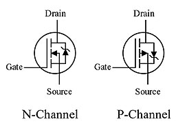
The purpose of a transistor is to switch on high voltage and current flow for high powered consumers e.g light bulbs in which the current flows the the collector to the emitter, using small amperage and voltage from the base to the emitter to switch on the high current flow from the collector. The transistor works a bit like a relay using small amperage to turn on high amperage.


Bipolar transistors are constructed of a three-layer semiconductor “sandwich,” either PNP or
NPN. As such, transistors register as two diodes connected back-to-back when tested with a
multimeter’s  “diode check” function as illustrated in the diagram below. Low voltage readings on the base with the black negative (-) leads correspond to an N-type base in a PNP transistor. On the symbol, the N-type material corresponds to the “non-pointing” end of the base-emitter junction, the base. The P-type emitter corresponds to “pointing” end of the base emitter junction the emitter.


Transistor Symbol and semiconductor construction shown below.

Identify the legs or terminals of the transistor with a multimeter.

Diode test (V) meter readings
Transistor number
VBE
VEB
VBC
VCB
VCE
VEC
NPN
 0.719v
 0.718v
O.L 
 0.715v
 O.L
 O.L
PNP
 0.683v
 O.L
 0.680v
 O.L
O.L 
O.L 


These readings are good as it shows that the transistor is working properly, if the transistor was showing open circuit (O.L) through out the test this would be a bad reading as this would indicate that the transistor has blown this could have been caused by overloading the transistor with to much current or to much voltage. The most likely place the transistor would have overloaded from on a NPN transistor is the base to the emitter, since the transistor acts like a relay using small current to switch on large current, the base to emitter could have had to small of a resistor and the switching side of the transistor could have had to much current and blown leaving the transistor useless.

EXPERIMENT No7

Transistor as a switch
Components: 1 x small signal NPN transistor, 2 resistors
Connect the multimeter between base and emitter.
Note the voltage reading and explain what this reading is indicating.

-The Voltage drop across the base to the emitter was 0.798 volts, this reading is good as its shows that the transistors switching side is working properly as this side of the transistor requires 0.7-0.8 volts to switch on the high power side or high current flow side of the transistor which flows from the collector to the emitter this allows for components like LED's or light bulbs to be switched on as they require high current flow. A bad reading would be O.L (open circuit) is it would indicate that the transistors switching side has blown which could have been caused by to much voltage or to much amperage and overloaded the transistors switching the side this would mean that the transistor would have to replaced.

Connect the multimeter between the collector and the emitter.
Note the voltage reading and explain what this reading is indicating.

-The voltage drop across the collector to the emitter was 0.054volts, this is a good reading as it shows that the switching side of the transistor is in the saturated region or is fully turned on with enough current flowing from the base to the emitter to effectively switch on the high power side of the transistor from the collector to the emitter, if the switching side of the transistor does not get adequate current flow then the high power/high current flow side of the transistor is not turned on properly. This means that there is a higher voltage drop across this area to keep current flowing kind of like a poor electrical connection that causes resistance to current flow, so the more current flow through the switching side of the transistor means more voltage and more current is able to flow through the high power side of the transistor as it has a stronger connection and less resistance so voltage and current can easily flow. Since the collector to the emitter acts as connection or wire there should be no resistance or little resistance to current flow so that the high power consumers can work properly. A bad reading would be one where there was high voltage drop as this means that the switching side of the transistor is not working properly and voltage is being used up to try and keep current flowing this means that the high power consumers such as LED's dont get enough voltage and current to work properly if at all as some of the supply voltage is being used up to get through the transistor. Another bad reading would be O.L (open circuit) as this would mean that the switching side of the transistor is faulty and will not allow current to flow from the collector to the emitter as it could have been overloaded. This would mean that the transistor would have to be replaced.


In the plot given below what are the regions indicated by the arrows A & B?


How does a transistor work in these regions? Explain in detail:
-The area that is marked A is the area when the transistor is known as being saturated or fully on, this means that there is enough current flowing from the base to the emitter to allow current to freely flow from the collector to the emitter. This means that there is no voltage drop across the collector and emitter as no voltage is required to keep current flowing through this area and the high powered consumers get the full current flow and voltage that they require. The area marked B is the cut-off area this means that there is not enough current flowing from the base to the emitter to allow current to flow from the collector to the emitter this basically means that the transistor is turned off so the circuit that the transistor is on is also turned off as current cannot flow through its circuit until the transistor is turned on

What is the power dissipated by the transistor at Vce of 3 volts?
-(Base to emitter) : P(power/watts)=V(volts)xI(current)
                               P = 3 x 0.005 = 0.015watts

-(Collector to emitter) : P = V x I 
                                       P = 3 x 0.013 = 0.039 watts


What is the Beta of this transistor at Vce 2,3 and 4 volts?
Beta=gain
Beta = Ic(current through collector)/Ib(current throught Base)
Beta = Ic/Ib

-    2 volts = 21mA/0.75mA = 28
     3 volts = 14mA/0.5mA = 28
     4 volts =  7mA/ 0.2mA = 35


EXPERIMENT no.8

Summary: Vary the base resistor and measure changes in voltage and current for Vce, Vbe, Ic and Ib. Then plot a load line.

Set up the following circuit on a breadboard. Use a 470R for Rc and a BC547 NPN transistor.


Pick 5 resistors between 2K2 and 1M for Rb. This is because you want a range of resistors that allow you to see Vce when the transistor is in the saturated switch region and when its in the active amplifier region.


  Record here:
 Rb 4.39v       Vbe  0.696v      Vce  0.697v       Ib 21.1 uA       Ic  5.37mA        (221k ohm's)
 Rb 4.689v     Vbe: 0.754v      Vce: 47.4mV     Ib: 461.6uA      Ic: 6.92mA         (1k ohm's)                        
 Rb 4.821v     Vbe: 0.668v      Vce: 2.444v      Ib: 8.3uA          Ic: 2.16mA         (560k ohm's)
 Rb 4.653v     Vbe: 0.757v      Vce: 43.7mV     Ib: 562uA         Ic: 6.95mA         (8.17k ohm's)
 Rb 4.716v     Vbe: 0.673v      Vce: 2.217v      Ib: 10uA           Ic: 2.60mA         (467k ohm's)


(uA=micro amps)


Discuss what happened for Vce during this experiment. What change took place, and what caused the change? 


-The different sized resistors at Rb meant that there was either more current flowing from the base to the emitter when the resistor is smaller, or less current flowing through the base to the emitter when a larger resistor is used. This will affect how well the transistor is switched on, if the transistor is not very switched on i.e. there is only a small amount of current flowing from the base to the emitter then this means that a voltage drop will occur across the collector to the emitter as there is resistance in the transistor and some voltage has to be used up in order to pass through the transistor. The greater the voltage drop the less switched on the transistor is and this means that the transistor is not in the saturated region when a voltage drop occurs, when there is a small voltage drop for this experiment it was 0.047volts as this circuit had the smallest resistor for Rb this means that the transistor is in a fully saturated or switched on region almost no voltage is required to keep current flowing through the circuit. But when the voltage was at 2.4 volts for this experiment it shows that the transistor was in the active region but it was not saturated so a large voltage is required to keep current flowing through the circuit. This change in voltage drop across the collector to the emitter was caused by the change in resistance at Rb, as more resistance to current flow was added through the base to the emitter the less current could flow this meant that the transistor could not operate in the saturated region. And voltage drops occurred

Discuss what happened for Vbe during this experiment. What change took place if any, and what caused the change?


-The voltage across the base to the emitter does not change very much as this part of the transistor is like a diode, and it only requires 0.6-0.7 volts to turn on the high powered side of the transistor from the collector to the emitter. However it would current flow through this part of the transistor that would be affected. This is a good reading as it shows that the switching side of the transistor is working properly, a bad reading would O.L (open circuit) as this would indicate that the transistors switching side has broken most likely from being overloaded, from to much voltage or to much amperage.

Discuss what happened for Ib during this experiment. What change took place, and what caused the change?


-Current flow through the base was affected by the size of the resistor used at Rb, if a larger resistor was used this means that there is more resistance to current flowing through the base so there is less current flow. When there is less current flowing through the base of the transistor this means that the transistor is most likely not in the saturated region and this means that a voltage drop would be occurring across the collector to the emitter to keep current flowing. When a smaller resistor was used at Rb there was less resistance to current flowing this meant that the transistor could be more saturated or switched on and there would be minimal voltage drop across the collector to the emitter. This means that there is more voltage and current available to the high powered consumers as it is not being used up in getting through the collector. These readings are all good as they show that the transistor is working properly and as expected. A bad reading would be one where there is no current flowing through the base, possibly caused by the transistor being overloaded with to much voltage or amperage. Another bad reading would be low amperage though the base even though a small resistor is being used this could indicate a faulty transistor that has poor connections and is causing internal resistance to current flow. In both cases the transistor would have to be replaced.


Discuss what happened for Ic during this experiment. What changes took place, and what caused the change?


-The change in size of resistors at Rb meant there was either more or less restriction to current flow through the base to the emitter. When a larger resistor is used this means that there is more restriction to current flowing through the base which means the transistor is not saturated or fully switched on and there is resistance to current flow in the collector hence the low amperage through the collector. However when a smaller resistor was used at the base this meant more current could flow through the base which meant that the transistor is more saturated or switched on and current could flow through the collector much more easily now. These readings are good as they where expected. Bad readings would be low amperage flow through the collector even if a small resistor is being used for the base, this would indicate a poor connection which is causing resistance and the transistor would have to be replaced.


Plot the points for Ic and Vce on the graph below to create a load line. Plan the values for so you use up the graph space.  Use Ic as your vertical value, and Vce as your horizontal value. Using Vbe on the Vce scale, plot the values of Ib.


Calculate the Beta (Hfe) of this transistor using the graph above.
-Beta = Ic/Ib
-Beta =6/0.2
-Beta=30


Explain what the load line graph is telling you. Discuss the regions of the graph where the transistor is saturated, cut-off, or in the active area.


-The load line is telling us the relationship between the current flowing through the base to the emitter and how that will affect the current flowing through the collector and what the voltage drop across the collector to the emitter will be. The saturated region of the transistor is on the left hand side of the graph from the top of the load line to just above the cut-off area from about 4mA and above on the Ic side. As this shows a low voltage drop across the collector to emitter. The transistor is saturated or fully switched on when the current flowing from the base to the emitter is above 0.4mA. The active region for the transistor is any area above the cut-off region, as this shows that there is current flowing through the base to the emitter but in most cases not enough to fully switch on the transistor and so there can be high voltage drops across the collector to the emitter. So this shows that the transistor is on but is not operating efficiently. The cut-off region is the area where there is not enough current flowing through base to the emitter to allow current to flow from the collector to the emitter. This means that transistor is off as no current can flow through the high power side of the transistor.


REFERENCE

http://www.tech-faq.com/wp-content/uploads/images/Resistor.jpg(resistor image)
 http://diyaudioprojects.com/Technical/Electronics/resistorcodes.jpg (resistor chart)
http://www.markallen.com/teaching/images/electronics/diode.jpg(diode symbols)
wiring diagram for experiment 2,3,4,7 and 8 from unitec labwork book
multimeter checking transistor image from unitec labwork book
transistor symbol and semiconductor construction image from unitec lab work book
transistor load line chart from unitec lab work book
http://www.cartft.com/image_db/1n4001.jpg(diode image)
http://9circuits.com/wp-content/uploads/wpsc/product_images/Red_led_x5-2.jpg(LED image)
http://upload.wikimedia.org/wikipedia/commons/e/e9/Zener_3D_and_ckt.png(zener diode image)
http://www.solarbotics.com/assets/images/cp3300uf/cp3300uf_pl.jpg(capacitor image)
http://www.opamp-electronics.com/catalog/images/MPS3904_40V_100mA_NPN_Switching_Transistor_007204.jpg(transistorimage)