.
BASIC ELECTRICS
First I'm going to talk about conventional electricity and electron theory, as these are major aspects to understanding electricity. Conventional current flow is when current flows from the positive power source for example a battery to the negative terminal of that battery, this is what is shown in all wiring diagrams. This is not correct as current or electrons actually flow from a negative terminal to a positive terminal, and this is known as electron theory or flow. However there is some truth to conventional current flowing from positive to negative as an atom especially good conductors i.e atoms with 1 or 2 electrons in the outer shell, leave positively charged holes in place of the electron, so spare electrons which are negatively charged, could jump from another atom to fill the spare hole and this happens to flow in the direction of conventional current flow from positive to negative. This has only recently been worked out as it was presumed that electricity flowed from positive to negative "In the 19th century, with the early applications of electricity such as starter motors and light bulbs, there was not an exact understanding of the nature of current flow. It was assumed at the time
that electricity flowed from the positive terminal to the negative." This is most likely the reason why wiring diagrams state that current flows from positive to negative, as it has been presumed that current flows this way for so many years that it would be to difficult to change and also that it easier to comprehend that current flows from positive to negative.
Now how to do calculations on a simple circuit.
 For this circuit, the amperage is going to worked out as the voltage supply is known and the resistance is known. The voltage current and resistance can be worked out using the triangle below.
Now how to do calculations on a simple circuit.


I=V/R
I=4.4v(this is because the diode requires 0.6v to turn on)/10 ohm's
I=0.44Amps.
You can also work out power dissapation across the diode using the equation triangle below.

So power dissapation across the diode = voltage x amperage so P=0.6v x 0.44amps
P=0.264 watts
and the power dissapation across the resistor would be P=0.44amps x 4.4v
P=1.936 watts
These are some easy equations to work out some of the different aspects of a electrical circuit.
VOLTAGE DIVIDER CIRCUIT
A voltage divider circuit, will provide a constant set voltage supply to a consumer that is always less than the supply voltage, for example if the power supply is 5volts, then a voltage divider circuit can supply a constant voltage of 3 volts to a consumer.

To work out what Vout is for the voltage divider circuit, you need to know what the resistors are in the circuit. So for example the resistors could be, R1=970 ohm's, R2=4700 ohm's, R3= 100 ohm's, the equation used to work out what Vout1 is Vout=R2 + R3/RT x Vin, so that would be Vout=4700 + 100/5770 x 12volts, this means that Vout 1= 9.98volts. Then to work out Vout2 that would be, Vout=R3/RT x Vin, Vout=100/5770 x 12, Vout2= 0.2 volts. These are the steps required to work out what the output voltages would be.
But if you want to pick what the voltage is for voltage divider circuit, for example you want a constant 4volts from a 5volt source for Vout1 and a constant 0.2 volts for Vout2 as an example. Then you would have to pick the first resistor(R1) and it can be any sized resistor, so for example a 1000 ohm resistor. Now you can work out the amperage is by calculating the voltage drop across the first resistor which would be 5volts-4volts=1volt, this means that I=V/R, I=1volt/1000 ohm's, I=0.001 amp. To work out what size the second resistor is (R2) you minus the available voltage by the voltage required at Vout2 this would be 4volts-0.2volts=3.8 volts and to work out resistance you divide voltage by current R=V/I, R=3.8volts/0.001amps, so R2=3800 ohm's. And to work out R3 is, the voltage required at Vout2 is divided by the current, R3=R=V/I, R=0.2/0.001amps, so R3=200 ohm's. This will then give a constant 0.2 volt supply from Vout 2.
OPERATIONAL AMPLIFIER
An operational amplifier(op amp) is a high gain electronic component(gain being the difference between the input and output voltages), the operational amplifier will take a small input voltage for example a 2volt input and can produce a higher output voltage for example 12 volts, or it can produce a negative or 0 volt when wired up as a comparitor but that will be explained later on. First the non-inverting op amp will be explained, the non-inverting op amp uses a small voltage input for the positive input side and produces a larger positive output voltage. This can be worked out using the equation Vout= ((Rf/Rs)+1)xVin, so if the input voltage is known and the resistors are known then Vout can be calculated.

INVERTING OP AMP
An inverting op amp works in a similar way to the non-inverting op amp except that the output is negative, the inverting op amp receives a small input voltage for the negative side of the op amps input, and if the op amps voltage rail is wired up to a negative voltage then the output would be a larger negative voltage than the voltage input. If the op amp is not wired up to a negative voltage and is only wired to ground or 0 volts then the output will be 0 volts. This circuit can be used as a negative switching circuit to switch components on and off on the negative side of the circuit. Whereas the non-inverting op amp can be used as a positive switchingcircuit. Vout can be worked out using the following equation, Vout=(Rf/Rs) x -Vin.
COMPARITORS
A comparitor is an operational amplifier that compares two input voltages and which ever is the biggest voltage will be the output. For example if there was a 2 volt source going to the inverting input and a 1.5 volt source going to the non-inverting input, then the output would be negative whatever the voltage is at the voltage rail. If these where switched around then the output would be a positive output to whatever the voltage rail is connected to, for example positive 12 volts. Here are some comparitor examples below.


MOSFETS
Mosfet's or metal oxide semi-conductor field effect transistors, are much like the normal BJT (Bipolar junction Transistor), in that both require a small input to switch on a larger output, and that both have two different types of transitors. The normal BJT has NPN and PNP and the MOSFET has a P-channel and a N-channel. However there are quite a few differences. For one the BJT is a current controlled device although there is a voltage drop that is required to switch on the transistor it is the amount of current that determines how well the transistor operates, in that a small amout of current is required flowing from the base to the emitter to switch on a larger current from collector to the emitter for a NPN transistor, a PNP transistor requires zero amperage to switch on. The MOSFET is a voltage controlled device in that for a N-channel FET(Field Effect Transitor), the more voltage that is applied to the gate (which is like the base on a BJT), the less resistance there is to voltage and amperage flowing from the drain to the source. However this is different for the P-channel FET , the more negative voltage that is applied to the gate the less resistance there is to voltage and current flowing, much like a PNP transistor.

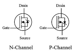
Within the to different channels for a MOSFET there are two different types of MOSFETs, there is the enhancement type, which is seen in the above image, this type of MOSFET "requires a Gate-Source voltage, ( VGS ) to switch the device "ON". The enhancement mode MOSFET is equivalent to a "Normally Open" switch." The other type of MOSFET is known as the depletion type MOSFET this type requires "the Gate-Source voltage, ( VGS ) to switch the device "OFF". The depletion mode MOSFET is equivalent to a "Normally Closed" switch." The depletion type MOSFET can be seen below.

Like the BJT the MOSFET also has a saturated region and a Cut-off region which are exactly the same for both MOSFETS and BJT's, in the saturated region the MOSFET has the correct amount of voltage at the gate to make it fully switch on. And when the voltage at the gate falls below a certain point then the MOSFET switches off, this is the cut-off region. The pros and cons of the MOSFET and BJT can be seen in the table below.
| Field Effect Transistor (FET) | Bipolar Junction Transistor (BJT) | |
| 1 | Low voltage gain | High voltage gain |
| 2 | High current gain | Low current gain |
| 3 | Very input impedance | Low input impedance |
| 4 | High output impedance | Low output impedance |
| 5 | Low noise generation | Medium noise generation |
| 6 | Fast switching time | Medium switching time |
| 7 | Easily damaged by static | Robust |
| 8 | Some require an input to turn it "OFF" | Requires zero input to turn it "OFF" |
| 9 | Voltage controlled device | Current controlled device |
| 10 | Exhibits the properties of a Resistor | |
| 11 | More expensive than bipolar | Cheap |
| 12 | Difficult to bias | Easy to bias |
The reason that the MOSFET is a voltage controlled device is that there is extremely high resistance at the gate of the MOSFET so there is almost no current flow through the gate to source, but this means that there is high amperage and voltage flowing from the drain to source. The MOSFET has an advantage over the BJT in that the MOSFET can handle much higher voltages and amperage than a BJT of the same size. However is seen in the chart above the MOSFET is easily damaged by static electricity that is generated by the body, the reason the MOSFET gets damaged is that the gate on the MOSFET acts like a capacitor and stores a charge in the gate, this damages the oxide in the gate and renders the MOSFET useless. To stop the MOSFET being damaged by static electricity, you must ground yourself when handling the MOSFET as this will stop static electricity accumulating on the body and damaging the MOSFET.
These are some of the basic electrical components that are used every day and the calculations that are required to work out the different vital aspects of an electrical circuit to make it work properly and effectively.
REFERENCE:
http://www.talktalk.co.uk/reference/encyclopaedia/hutchinson/m0030248.html(conventional current flow quote) http://www.electronics-tutorials.ws/dccircuits/dcp24.gif(power triangle)
http://www.markallen.com/teaching/images/electronics/comparator.jpg(comparitor image)
http://www.acdcshop.gr/img/components/transistor_fet/fet/3197_irfp4227pbf.jpg(mosfet image)
http://simreal.com/mediawiki/images/2/26/Fig06-02.jpg(P and N channel MOSFET enhancement image)
http://www.electronics-tutorials.ws/transistor/tran_6.html(quote for enhancement type MOSFET)
http://www.electronics-tutorials.ws/transistor/tran_6.html(quote for depletion type MOSFET)
http://electricalandelectronics.org/wp-content/uploads/2008/09/symbol-of-depletion-type-mosfet.png(depletion MOSFET Image)
http://www.electronics-tutorials.ws/transistor/tran_8.html(BJT/MOSFET comparison table)
Excellent work Richard! Full marks
ReplyDelete